Silicon Photonics vs Indium Phosphide — The Foundry War Behind Your Optics
Two materials. Two manufacturing ecosystems. Two different bets on the future of optical networking. The choice between Silicon Photonics and Indium Phosphide determines who can build your optics, how fast, at what cost, and with what performance ceiling.
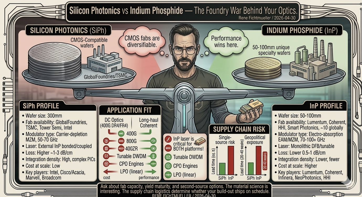
Silicon Photonics (SiPh) uses standard CMOS fabrication processes to build optical components on silicon wafers. The same fabs that produce CPUs and memory chips can produce photonic circuits. Modulators, waveguides, and detectors integrate onto a single silicon die.
The catch: silicon cannot emit light. You still need an external laser, typically made from Indium Phosphide, bonded or coupled to the silicon chip. Every SiPh module contains an InP component. The question is how much integration you can push onto silicon before hitting physics limits.
Fab availability GlobalFoundries, TSMC, Tower Semi, Intel
Modulator type Carrier-depletion Mach-Zehnder (MZM)
Modulation bandwidth 50–70 GHz (improving, but lags InP)
Laser External InP laser required (bonded or edge-coupled)
Loss Higher waveguide loss than InP (~1–3 dB/cm)
Integration density High — complex PICs with hundreds of components
Cost at scale Low — CMOS-compatible volume manufacturing
Key players Intel, Cisco/Acacia (Luxtera heritage), Marvell, Broadcom
Indium Phosphide (InP) is a III-V semiconductor that emits, modulates, and detects light natively. A single InP chip can contain the laser, modulator, and photodetector. No external laser required. No bonding step. One material does the entire photonic job.
The trade-off: InP fabrication uses small wafers (50–100 mm), specialized equipment, and a limited number of fabs worldwide. Yields are lower. Cost per die is higher. But raw photonic performance exceeds silicon in bandwidth, power efficiency, and optical loss.
Fab availability Lumentum, Coherent (II-VI), HHI, Smart Photonics, ~10 globally
Modulator type Electro-absorption (EAM) or MZM — monolithic
Modulation bandwidth 70–100+ GHz
Laser Monolithic — DFB, tunable, no external source needed
Loss Lower waveguide loss (0.5–1 dB/cm)
Integration density Lower — fewer components per PIC than SiPh
Cost at scale Higher — specialty fab, small wafers, lower yield
Key players Lumentum, Coherent, Infinera, NeoPhotonics (acquired), HHI
Short-reach data center optics at 400G and 800G: SiPh dominates on cost. CMOS fabs produce millions of photonic dies per year. The volume curve bends cost down in ways that InP fabs cannot match. Intel ships SiPh-based 400G DR4 and FR4 modules at scale.
Coherent optics for metro and long-haul: InP leads on performance. DP-16QAM modulation at 64+ GBaud needs bandwidth and linearity that InP modulators deliver natively. Acacia (now Cisco) uses SiPh for coherent, but hybrid-integrates InP lasers and pushes the silicon modulator harder to compensate for its bandwidth disadvantage.
800G DR8/FR4 (DC) SiPh — same logic, higher integration
400ZR/ZR+ (DCI) Both — SiPh (Acacia) vs InP (Lumentum, Coherent)
Long-haul coherent InP — performance ceiling matters
Tunable DWDM InP — native tunable laser integration
CPO engines SiPh preferred (CMOS integration with ASIC)
LPO (linear) Both — laser source is the differentiator
SiPh modules depend on CMOS fabs for the photonic circuit and InP suppliers for the laser. If a laser supplier has a capacity constraint, SiPh modules cannot ship regardless of how many silicon PICs sit in inventory.
InP modules depend on a smaller set of fabs. A fire, earthquake, or capacity reallocation at one InP foundry can constrain the global supply of coherent optics for quarters. This happened. It will happen again.
InP wafer fabs ~10 globally (specialty, concentrated)
InP laser supply Critical for BOTH platforms (SiPh needs external laser)
Single-source risk InP: high | SiPh: moderate (laser bottleneck)
Geopolitical exposure InP fabs concentrated in US, Europe, Japan
Lead time under stress InP: 20–40 weeks | SiPh: 12–20 weeks
Dual-sourcing across both platforms is the only hedge that works. If your coherent optics come from a single vendor on a single material platform, you carry concentration risk that procurement spreadsheets do not capture.
The clean "SiPh vs InP" framing is already obsolete. Cisco/Acacia bonds InP lasers onto SiPh PICs. Intel is developing integrated InP-on-silicon processes. Heterogeneous integration, combining the best of both materials on a single package, is where the industry is heading.
Your vendor's material platform matters less than it did three years ago. What matters is whether they can deliver at the volume and lead time your deployment requires. Ask about fab capacity, yield maturity, and second-source options. The material science is interesting. The supply chain logistics determine whether your build-out ships on schedule.